|
Price:
( Exclude shipping cost)
Standard version: USD1830
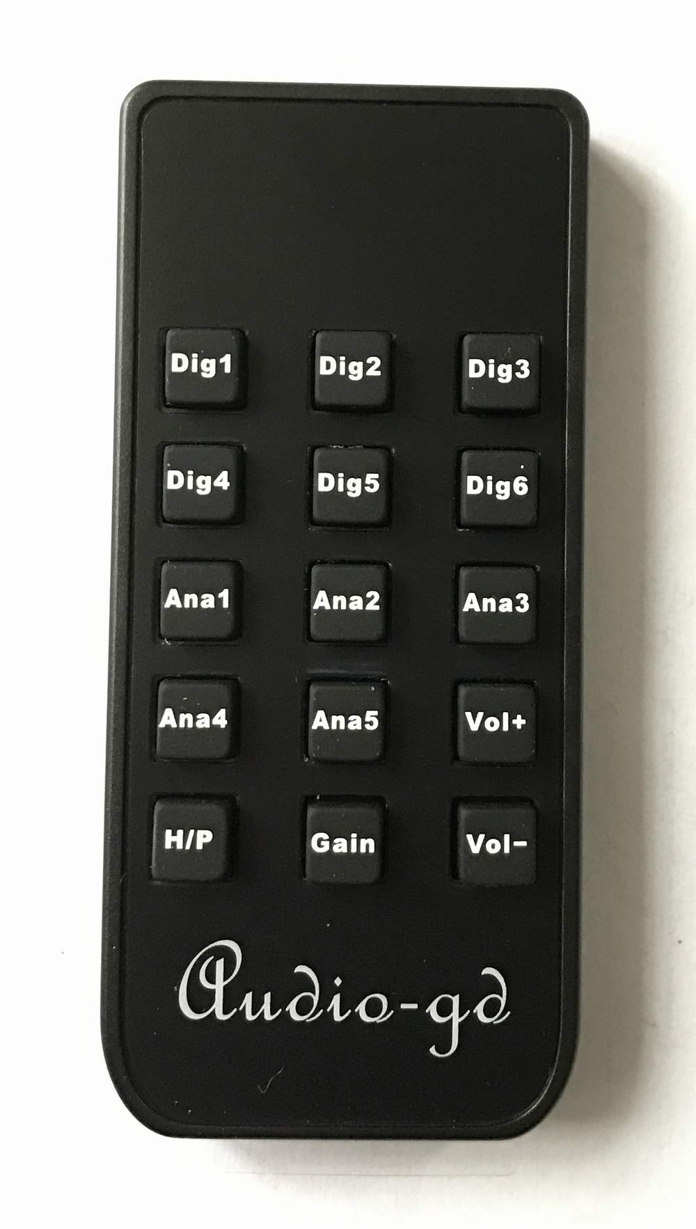
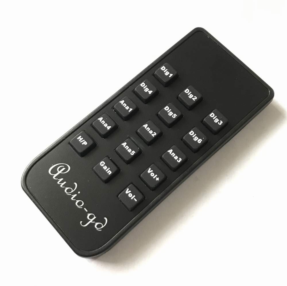
(Free mini remote ,non
warranty.)

Full upgrade version: USD1990
Below upgrade options
had included in the Full upgrade version:
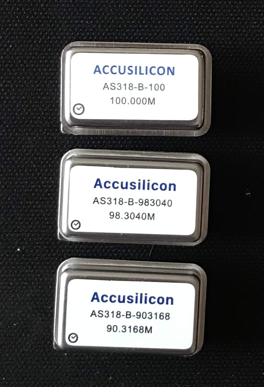
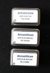
1, Upgrade Femtosecond
Accusilicon *2 Femtosecond clocks,
2, Upgrade Crystek *2
on USB interface,
3, Upgrade USB interface with isolator and separate PSU,
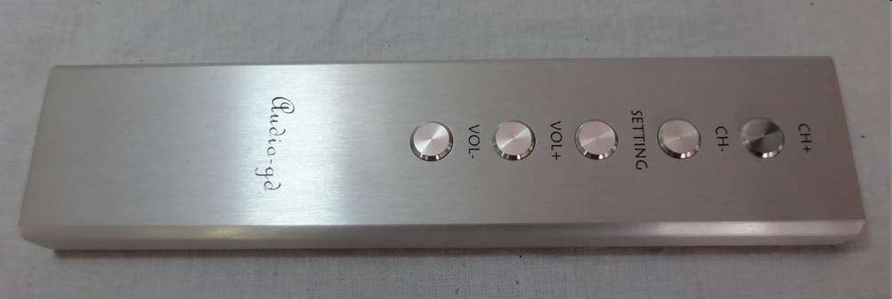
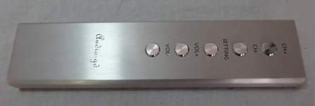
4, Upgrade mini remote to metal remote.)
Please send your address, name
to audio-gd@vip.163.com
get the quote.
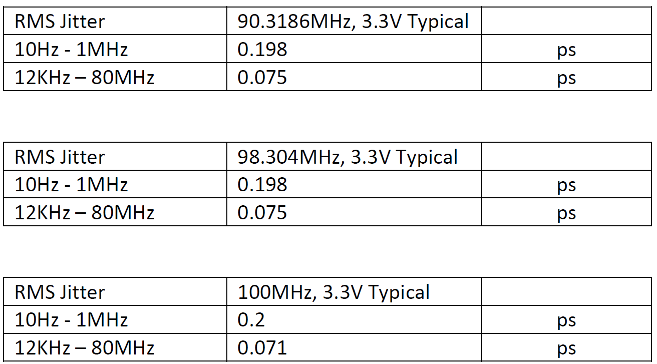
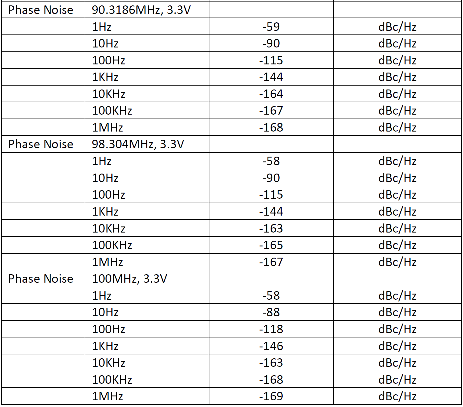
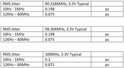
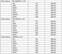
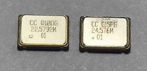
Accusilicon clocks:
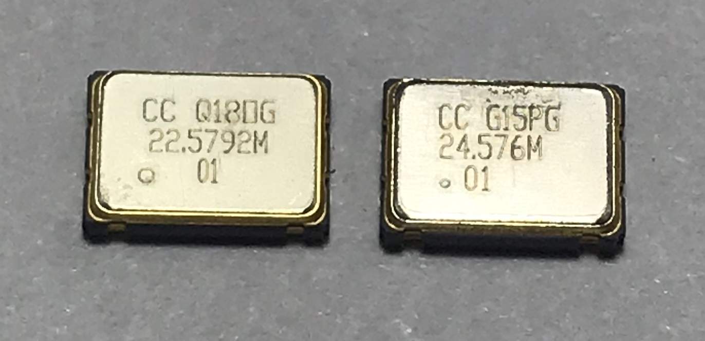
Crystek clocks:
Click to download the
driver of
Amanero
combo 384
Pros and cons of R-2R DAC :
Advantages:
1.R-2R will not convert the clock signal into the output
signal.
2. R-2R is not sensitive to jitter .Delta-Sigma D/A is much
more sensitive to jitter.
3. The output signal is much more precise compared to
Delta-Sigma D/A .
Weaknesses:
1.THD today is extremely good with Sigma Delta chips in
comparison to R2R ladders are good too but not as good.
2. Glitches and accuracy of the ladder resistors are very
difficult to avoid and require complex technology to resolve it.
R-2R basic design in the market:
The
R-2R DAC is very popular nowadays and available from DIY kits up to
completely high-end products.
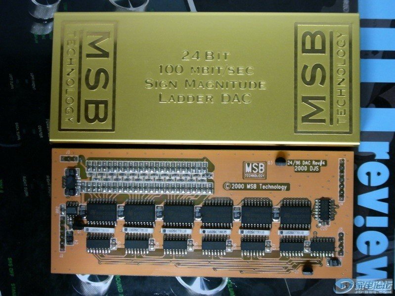
In the low range DIY market, the R-2R design is often
based on old technology designed a long time ago by MSB and only
includes basic R2R ladder design and do not include the wonderful
correction design of the original MSB technology. This design uses
data shift registers logic chips in series mode to convert the data
to an analog signal. The structural R2R technology issues cannot be
avoided, and performance is solely depending on the accuracy of the
ladder resistors.
In the High-End market the R2R design is much more complex and
achieves better performance. A basic R2R ladder is simply not
sufficient enough to achieve good performance and high sound
quality! Some manufacturers are using shift registers design. A less
complex and less efficient design based on traditional logic chips
working in serial mode to correct the ladder.
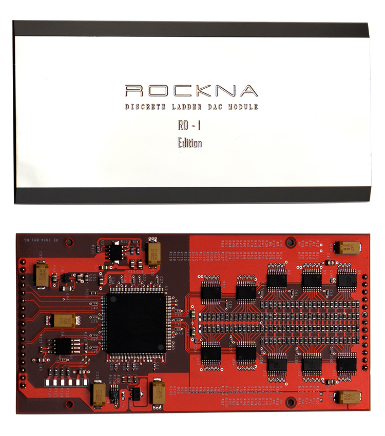
A far better design switches resistors in parallel mode. An
ultra-fast FPGA controls and corrects the R2R ladder. The parallel
design mode controls every bit respectively and therefore achieve
unprecedented performance. (In parallel mode only 1 clock cycle is
needed to output all data; serial design mode needs at minimum 8 up
to 24 clock cycles) The parallel design is much more complicated.
Once designed properly it can correct every bit of the ladder.
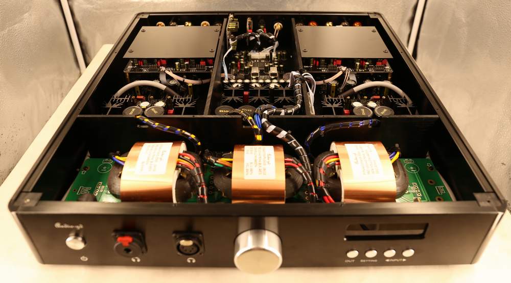
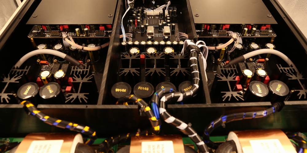
Photo below shows a design with such FPGA, can correct the
unavoidable imperfections of the R2R ladder caused by intolerance of
resistors glitches and achieve best performance.
Accuracy of the ladder resistors (tolerance):
Many
people believe the tolerance of the resistors in the ladder is most
important to reach best performance. Nowadays 24 bit resolution is
standard. What tolerance is needed to achieve 24 bit resolution?
When we look at 16 bit the tolerance of 1/66536, 0.1%
(1/1000) is far not enough, even a tolerance of 0.01% (1/10000), the
best tolerance available in the world today, still cannot handle 16
bit correctly; we are not even calculating 24 bit here!
The tolerance of the resistor will never solve
Imperfections of a ladder. This would require resistors with a
tolerance of 0.00001% and ability to handle 24 bit resolution. This
is only in theory because the discreteness of the switch logic chips
have already too much internal impedance and will destroy the
impossible tolerance of a the resistor.
The solution is to correct the ladder and not to depend
on the tolerance of resistors. It’s a combination of both: Ultra-low
tolerance resistors controlled by a correction technology and very
high speed FPGA which is applied in in our design.
Importunacy of the FPGA :
FPGA
stands for Programmable Array Logic.
Nowadays the FPGA is applied in a lot of high end DACs;
like the popular ROCKNA WAVEDREAM DAC.
The internal hardware design is fully controlled by
complex software. A huge advantage is the fact that the software in
the FPGA can easily be upgraded offering new features or improve the
performance. Such design is much more flexible and future proof!
FPGA tasks
The
FPGA is responsible for:
1. High performance SPDIF interface, replacing
traditional less good performing SPDIF interface chips like DIR9001,
WM8805 or AK411X,etc.
2. Full re-clocking process with FIFO design applicable
on all inputs. This way the output data keeps fully synchronized
with the clock signal to reject any jitter.
3. Built in 2X, 4X and 8X oversampling and digital
filters and on top of this 4 different true NOS (only analog 6dB
filtering) modes. To completely configure it to your liking!
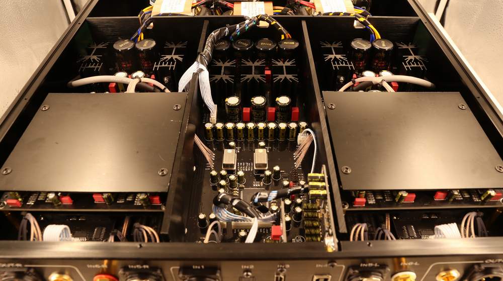
Built in an excellent real balance discrete amp
The
signal last stage is the analog output stages, which have paramount
effect the final DAC sound quality.
After d/a conversion by the R2R D/A modules the analogue
signal is transported by fully discrete matched-transistor output
stages.
The high speed special ACSS output stages are non-feedback
and current driven design.
They are Special because almost all other designs need to
convert the signal multiple times from and to current or voltage,
resulting in less detail and less defined soundstage .
The
output stages have built in 4 pair 15W transistors to offer strong
drive capanility .The diamond differential design can avoid switch
distortion , it is working in a class A but don't draw large
current while idle . The balance drive mode can kill the noise and
distortion and improves the soundstage presentation ,background and
the transparency ,ect.
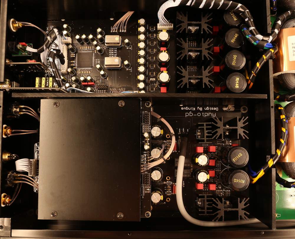
Full discrete class A Headamps and Preamps
that is same design with the Master 9:
The
signal last stage is the analog output stags , they greatly effect
the whole DAC sound
quality.
The native
advantage of the ACSS design, the DA output signal only through 1
stage gain stage ,it is non feedback design and working in current
signal mode, keep the sound coloration least and sound most like
real.
The output buffers are the pure class A design , built
with 8 pcs 150W
(in total 1200W ) , to drive the most headphones
without difficulty .
In our design output stages working in pure class A ,
and without any negative feedback for the most pure and life like
sound reproduction .
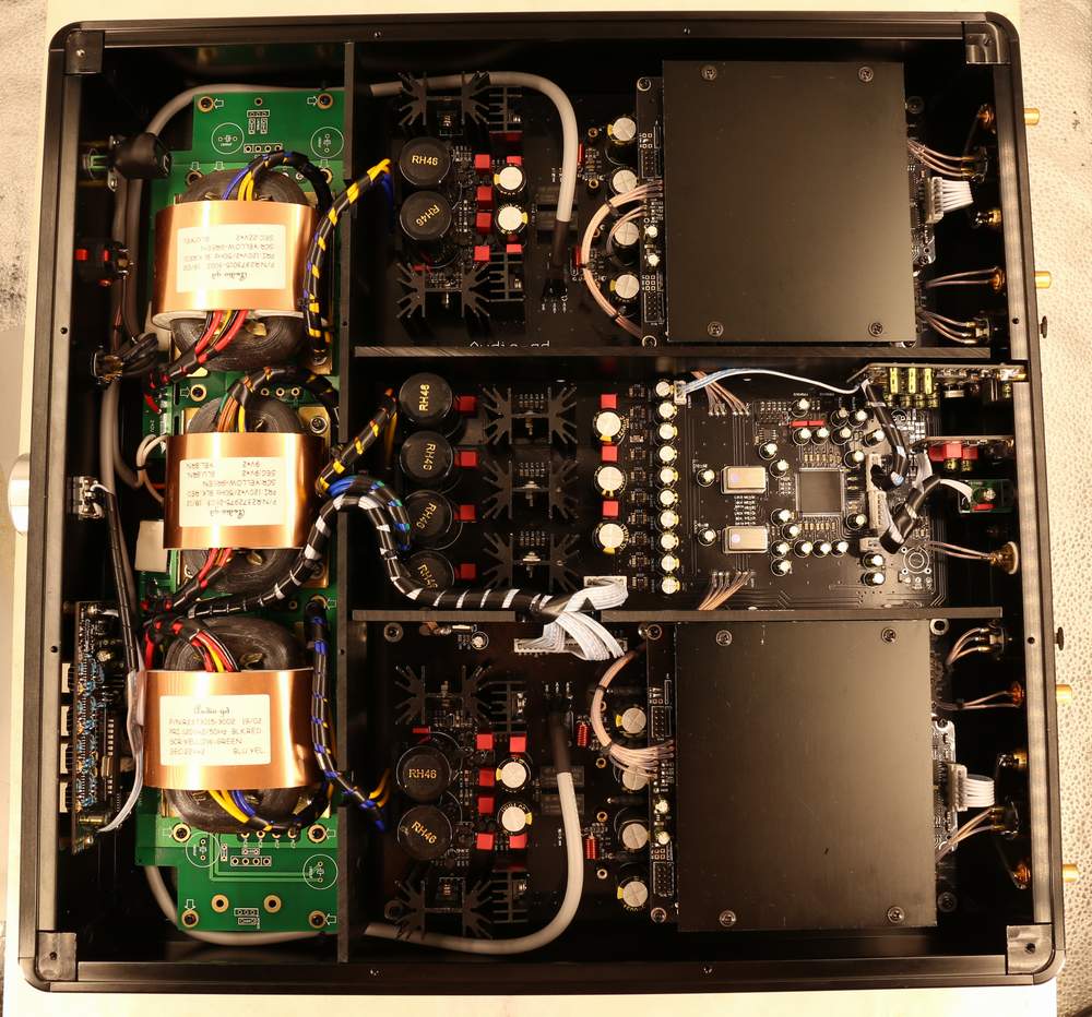
Heavy power supplies design:
The
DAC has the high quality low noise, low flux leakage, R-cores
transformers to supply all digital parts as well as left and right
analog boards.
There are 3 unit R-cores for power supply digital parts and Left/
Right parts separately , in total the R-cores power is 135W.
There are in total 14 groups ultra-high speed and
ultra-low noise PSUs built in and applied in a double stage PSUs
technology for stable power delivery. That design allowes get very
clean power supply for the digital parts of DAC.
There are
4 groups of pure class A PSUs built in for
the analog amps .
|