|
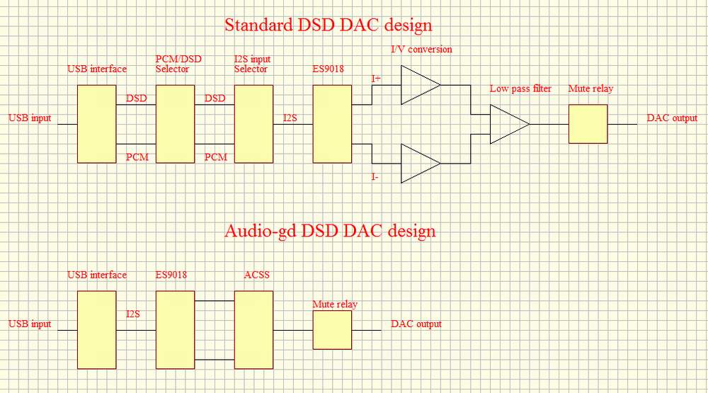
Simply describe DSD DAC design The standard DSD DAC design as below picture. The USB interface chip output I2S signal, through the DSD flash control the output selector chip, separate the PCM and DSD I2S signals , feed to the I2S input selector chip . The ES9018 had the current audio signal + and -, separately through two OPAs ( in one channel ) implement the I / V conversion , then feed to the low pass filter OPA and output . On the output point, a relay implement mute design, for mute the DSD and PCM switch noise . This is necessary , the ES9018 had different configure state for working with DSD and PCM , so switch between PCM and DSD will had the switch noise output.
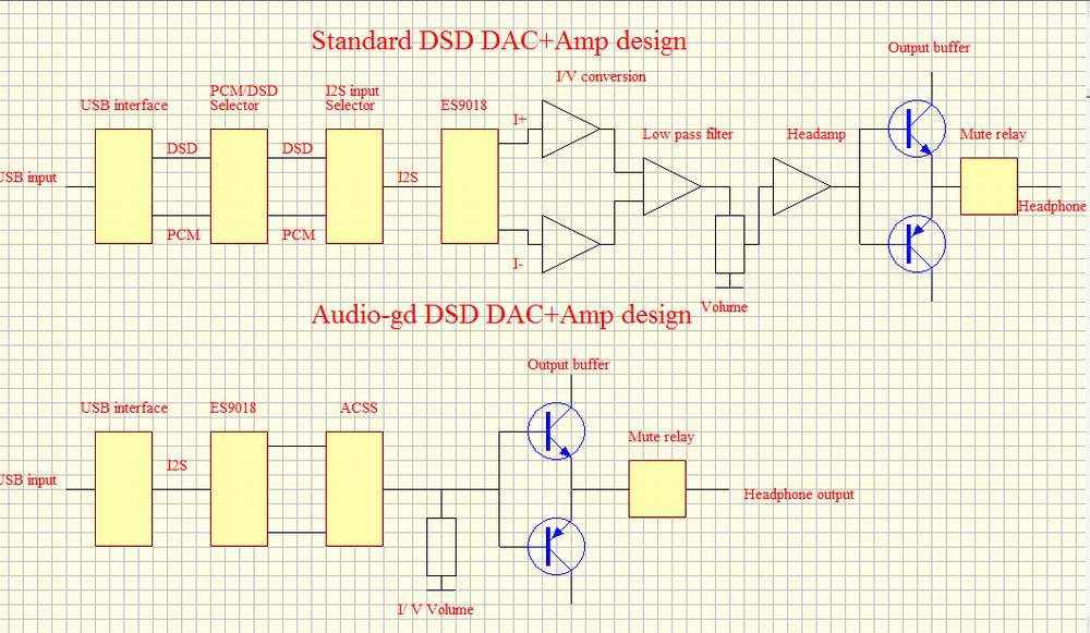
In audio-gd design, we follow the rule, the signal journey simple and short is best for neutral sound . The USB interface chip output I2S can auto configure for DSD output or for PCM output, so we don’t need the PCM / DSD output selector and the I2S input selector , the USB interface chip feed to the ES9018 direct . The ES9018 had the current audio signal + and – output, this is the best match with the ACSS design, the ACSS design working on current signal , so don’t need the I/V conversion after the ES9018 . The CAST design had built in the I/V conversion and low pass filter on output point, through the mute relay for mute the DSD and PCM switch noise. Below is the DSD DAC with amp design .
|
|
备案序号: 粤ICP备05020367号 版权所有: 睿志音响 Copyright(C) 2004 www.audio-gd.com All Rights Reserved |